ホワイトペーパー
September 17, 2025
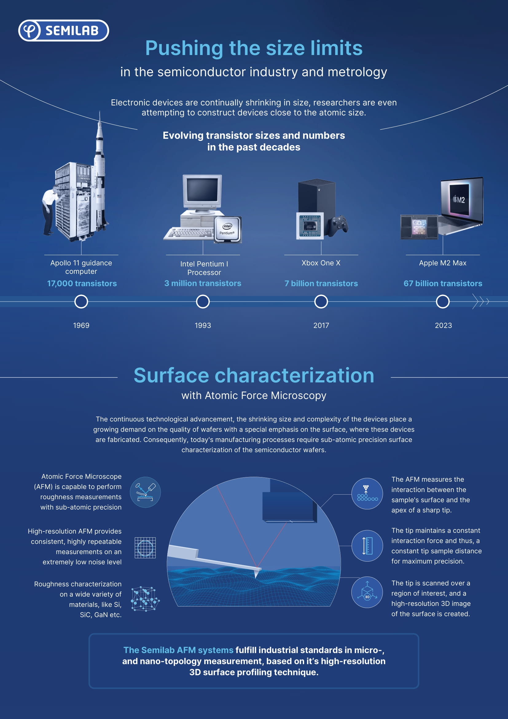
Pushing Size Limits in the Semiconductor Industry and Metrology
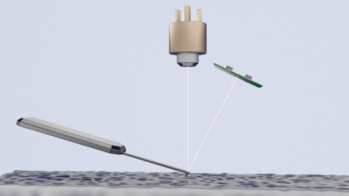
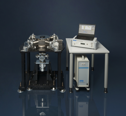
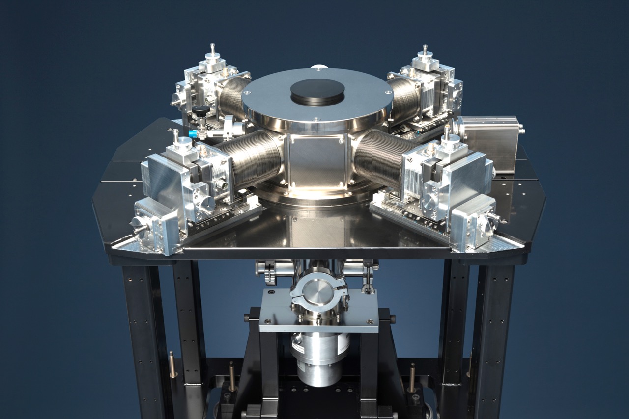
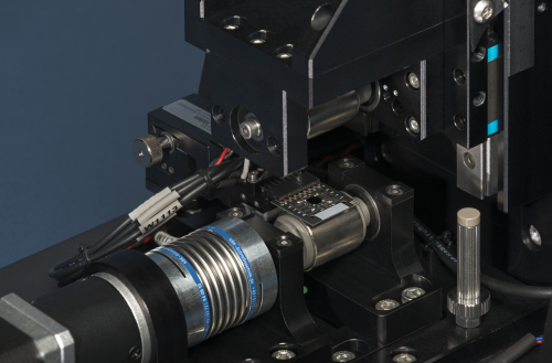
Unlock the true potential of AFM with the Semilab AFM product family, elevating your understanding of materials for research and manufacturing excellence. Meet our newest addition, the AFM-3000.
September 17, 2025
Tailored Surface Characterization Tools for R&D
Exploring how tailored surface characterization tools enhance R&D by boosting material insights, productivity, and competitive advantage.
November 26, 2025
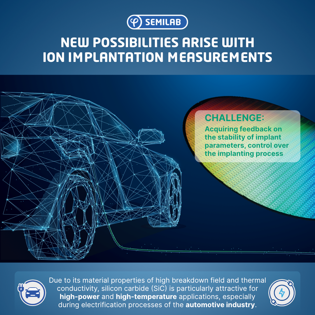
Driving Innovation in Power & Automotive industries with Ion Implantation Measurements
In the Power and Automotive industries, one of the biggest challenges is ensuring stable implantation parameters and precise control over the implantation process. These challenges are especially critical in the electrification era.

September 23, 2025
From GaAs to SiC: Measuring Resistivity in Compound Semiconductors
Discover why accurate resistivity measurement is the key to unlocking the full potential of compound semiconductors in powering the future of energy, mobility, and high-frequency technologies.
February 5, 2026
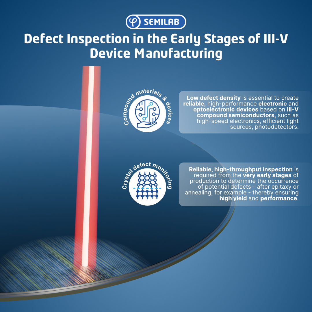
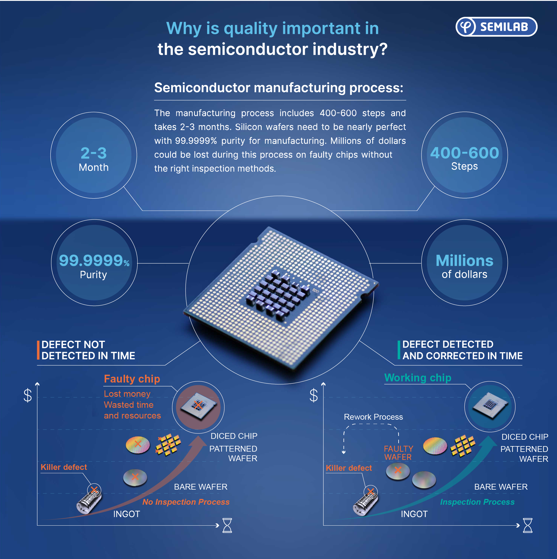
Defect Inspection in the Early Stages of III-V Device Manufacturing
In the world of III-V compound semiconductors, performance starts long before devices ever reach final test. Whether powering high-speed electronics, enabling efficient light sources, or driving advanced photodetectors, these materials demand exceptional crystal quality from the very first processing steps.
August 18, 2025
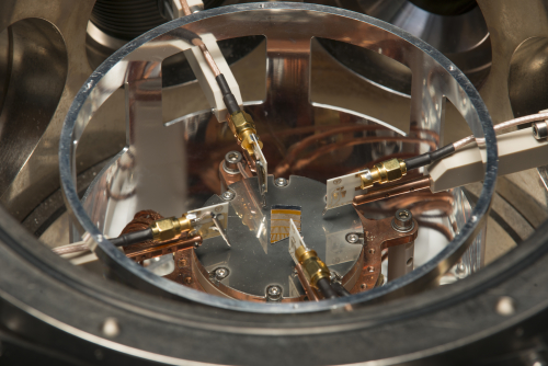
Interpreting QD Properties with Deep-Level Transient Spectroscopy
Uncover the intricacies of your semiconductor samples with precision and confidence and join us in shaping the future of quantum dot technologies and semiconductor excellence.
August 18, 2025
What You Need To Know About Using Deep Level Transient Spectroscopy In Semiconductor Manufacturing
Semilab provides DLTS solutions with over 30 years of global experience.
August 18, 2025
AC vs. DC Magnetic Field Measurements: Understanding Techniques and Applications
Learn about the distinctions between AC and DC Hall measurement techniques and how the Semilab PDL Hall system provides a versatile solution for characterizing electronic materials and devices.
August 18, 2025
About the Importance of Quality Control in the Semiconductor Industry and the Possibilities of the Light Scattering Tomography Technique
Spot bulk micro defects early with Semilab’s advanced light scattering tomography system for flawless silicon wafers and better chip yield.
August 18, 2025
Deep-level Transient Spectroscopy for Wafer Inspection
DLTS offers unmatched sensitivity for detecting and analyzing defects in semiconductors, making it a powerful tool for advanced wafer characterization.
August 18, 2025
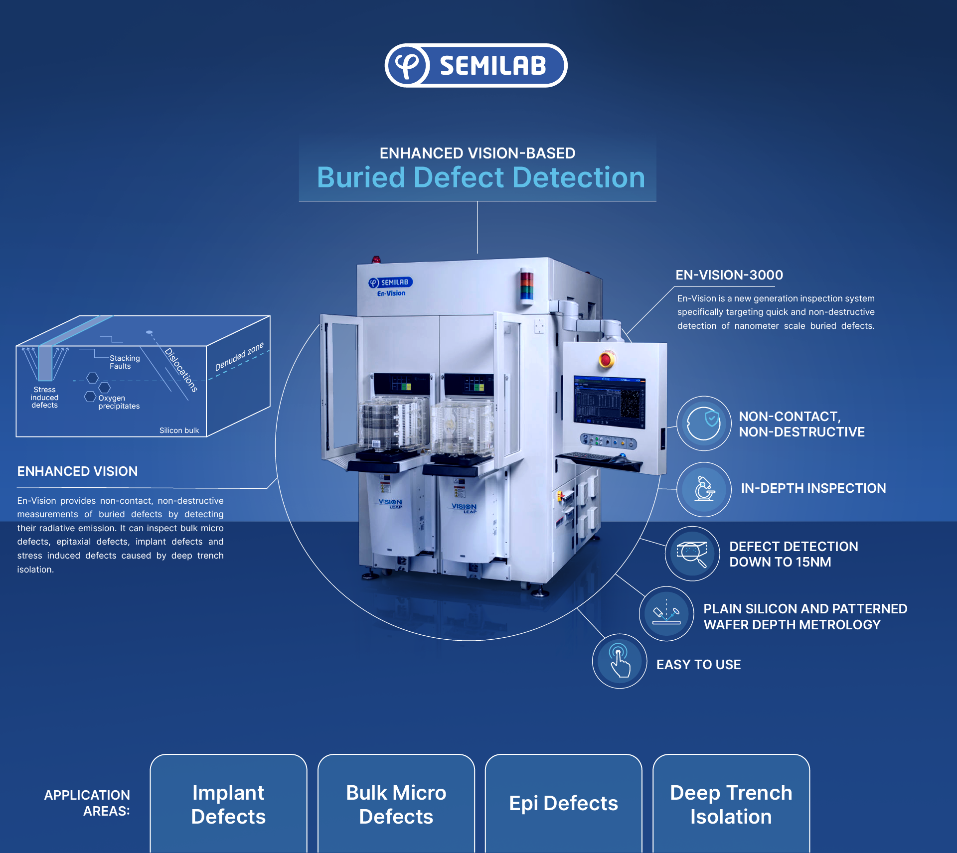
Enhanced Vision – Enhanced Defect Detection
Explore the Semilab En-Vision system's unique capabilities, applications, and benefits.
August 18, 2025
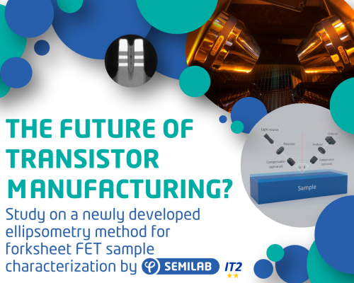
Forksheet FET - the Future of Transistor Manufacturing?
Semilab, within the IT2 EU project, explores Mueller matrix ellipsometry as a powerful method to detect asymmetries in forksheet FETs—offering enhanced precision over conventional techniques and supporting Europe's push for semiconductor innovation.
August 18, 2025
How Does Advanced Metrology Benefit the PV Industry?
Explore how advanced metrology plays a crucial role in the photovoltaic industry by enhancing efficiency, ensuring quality control, supporting research and development, and reducing costs.
August 18, 2025
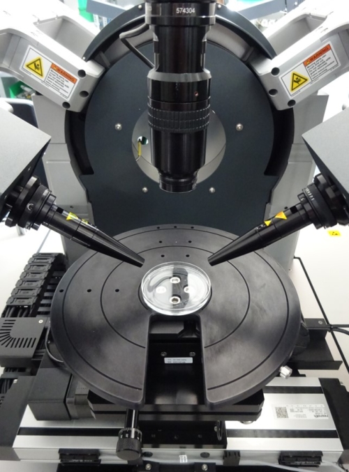
How Spectral Ellipsometry Measurements are Conducted on Bulk Liquids
Enabling precise optical characterization of bulk liquids using advanced spectral ellipsometry despite interface instability.
August 18, 2025
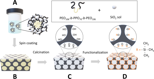
How to Determine the Internal Wettability of Nanostructured Thin Films
Advancing wettability analysis of nanostructured thin films with ellipsometric porosimetry and spectral ellipsometry.
August 18, 2025
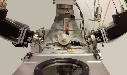
Precision Measurement Tools for the Sub-Nanoscale
Real-time in situ spectroscopic ellipsometry reveals key insights into sub-nanoscale growth of molybdenum carbide thin films.

August 18, 2025
R&D Lab Tools for the Display Industry
Innovation in the electronic display industry is driven by advanced R&D tools enabling precise measurement and development.
August 18, 2025
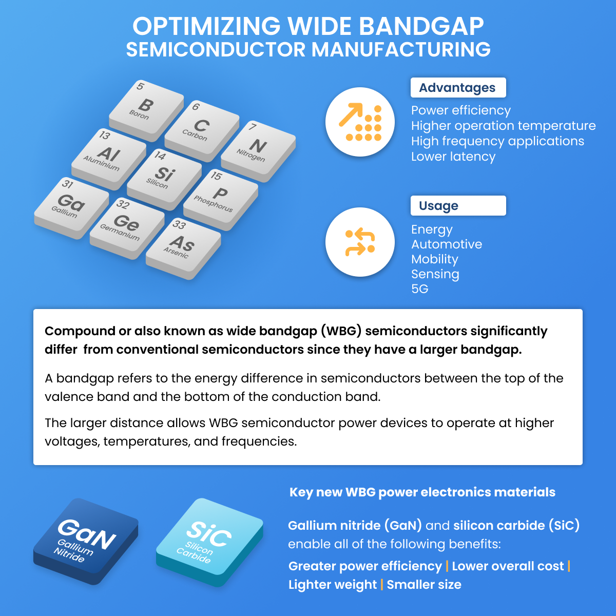
Wide Bandgap Semiconductors, Their Most Common Industry Usage and What Semilab Can Offer for Compound Material Characterization
Driving the future of power electronics: Explore how Semilab’s Metrology tools optimize GaN and SiC performance.
October 17, 2025
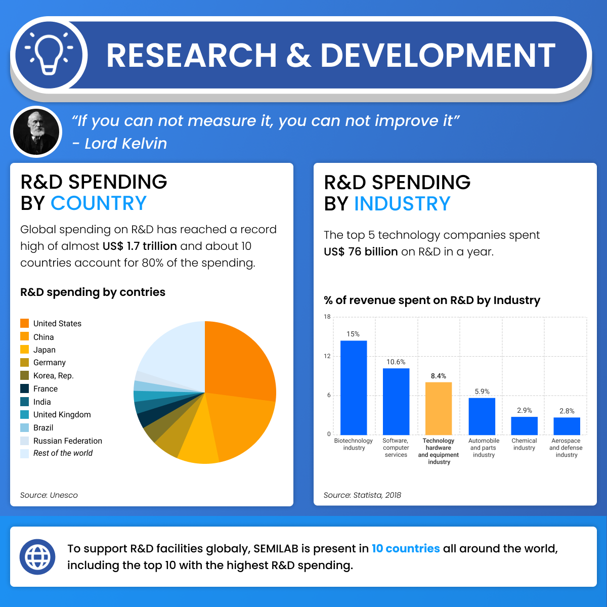
R&D Keeps The World Moving Forward - So Are Semilab’s Spectroscopic Ellipsometry Solutions
Technological development is transforming every aspect of our lives and our world at an unprecedented rate, and Semilab proudly contributes to this incredible pace.
October 17, 2025
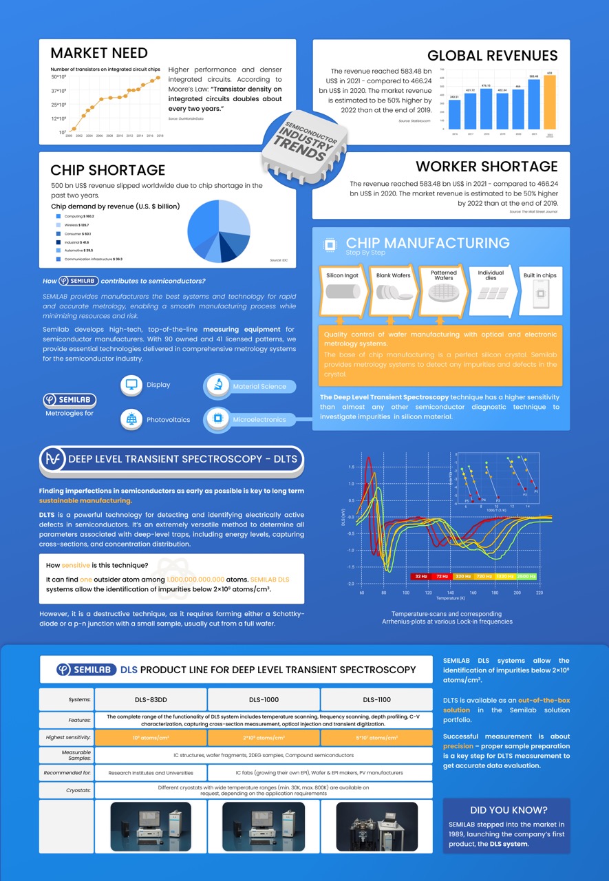
The Latest Semiconductor Industry Trends And Semilab’s Contribution To The Market
Meeting rising chip demand with precision: How Semilab’s Advanced Metrology takes on complexity in semiconductor manufacturing.