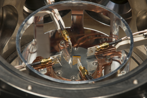
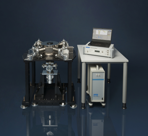
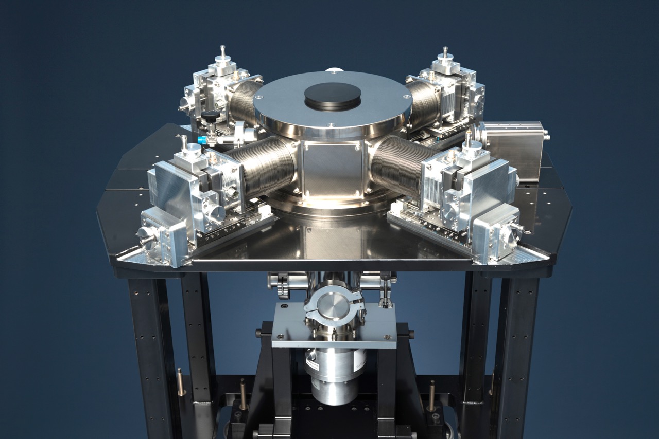
DLS-1100 Deep Level Transient Spectroscopy
The DLS-1100 is a high-end DLTS system designed for semiconductor R&D and production environments. Featuring an external cryostat for precise temperature control, it offers top-tier sensitivity, full automation, and advanced customization — ideal for production labs, foundries, and high-throughput research facilities.
関連出版物
Analytical Tools for the Characterization of Power Devices
Ballistic Electron Emission Microscopy of Schottky Diodes on RF-Plasma-Treated Silicon
DLTS Investigation of Deep Levels in Bulk GaAs under Uniaxial Stress
Diffusion of Iron in Silicon Dioxide
Homogeneous Transparent Conductive ZnO:Ga by ALD for Large LED Wafers
Interpretation of the Electric Field Dependent Thermal Emission Data of Deep Traps
Investigation of Deep Levels and Precipitates Related to Molybdenum in Silicon by DLTS and Scanning Infrared Microscopy
NIST Traceable Small Signal Surface Photo Voltage Reference Wafer
Quantitative shear stress imaging in high throughput in-line Si wafer inspection
Temperature Dependence of the Capture Cross Section of Seo as Measured by Microwave Absorption Spectroscopy (MAS)
Three Dimensional Mapping of Thermal and Tunneling Electron Emission from InAs/GaAs Quantum Dots
関連ホワイトペーパー
August 18, 2025
Deep-level Transient Spectroscopy for Wafer Inspection
DLTS offers unmatched sensitivity for detecting and analyzing defects in semiconductors, making it a powerful tool for advanced wafer characterization.
August 18, 2025
Interpreting QD Properties with Deep-Level Transient Spectroscopy
Uncover the intricacies of your semiconductor samples with precision and confidence and join us in shaping the future of quantum dot technologies and semiconductor excellence.
October 17, 2025
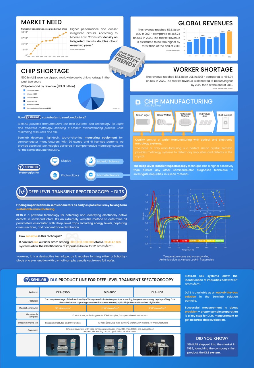
The Latest Semiconductor Industry Trends And Semilab’s Contribution To The Market
Meeting rising chip demand with precision: How Semilab’s Advanced Metrology takes on complexity in semiconductor manufacturing.
August 18, 2025
What You Need To Know About Using Deep Level Transient Spectroscopy In Semiconductor Manufacturing
Semilab provides DLTS solutions with over 30 years of global experience.