physica status solidi (a) - applications and materials science2022
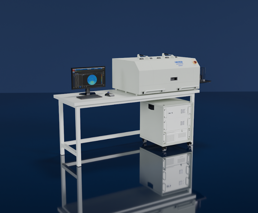
Characterization of AlXGa1−XN/GaN High Electron Mobility Transistor Structures with Mercury Probe Capacitance–Voltage and Current–Voltage
Author: Eric Tucker, Frank Ramos, Samuel Frey, Robert J. Hillard, Péter Horváth, Gyula Zsákai, Attila Márton
Topic: dielectric characterization; dielectric charge; MERCURY C-V PROFILING; 2DEG sheet charge; pinch-off voltage; mercury gate
Read publication