November 26, 2025Driving Innovation in Power & Automotive industries with Ion Implantation Measurements
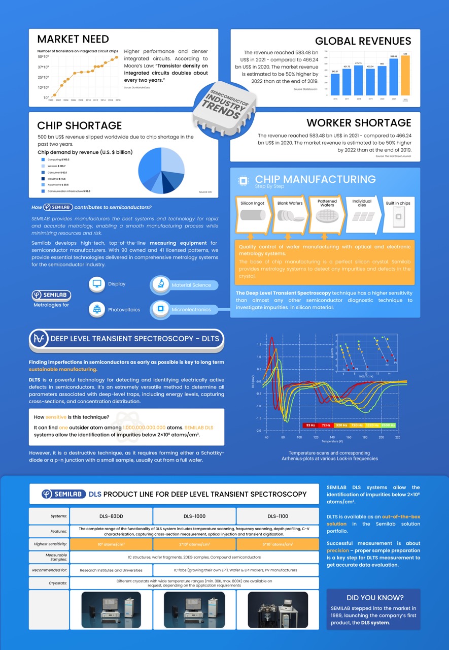
August 18, 2025What You Need To Know About Using Deep Level Transient Spectroscopy In Semiconductor Manufacturing
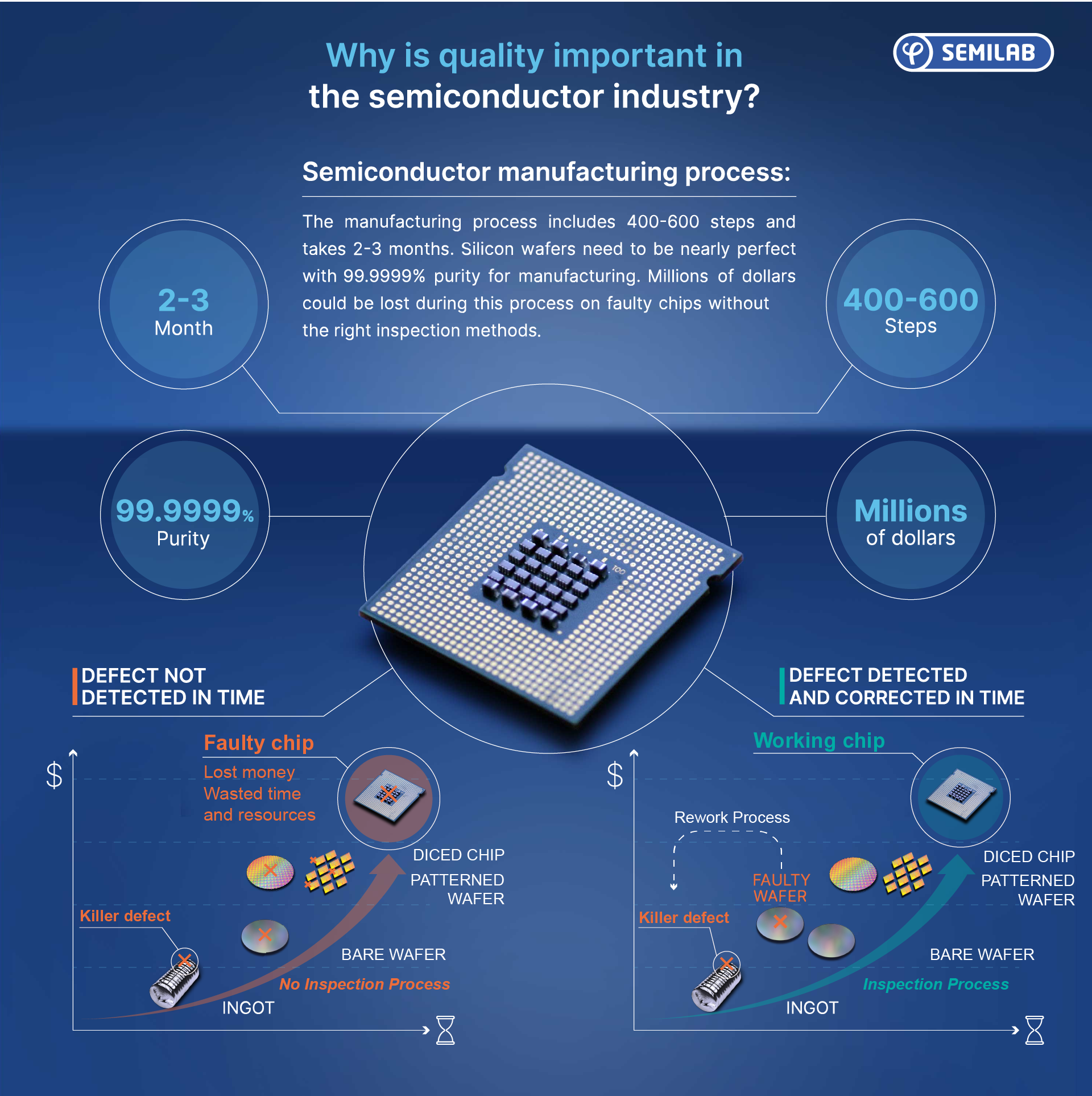
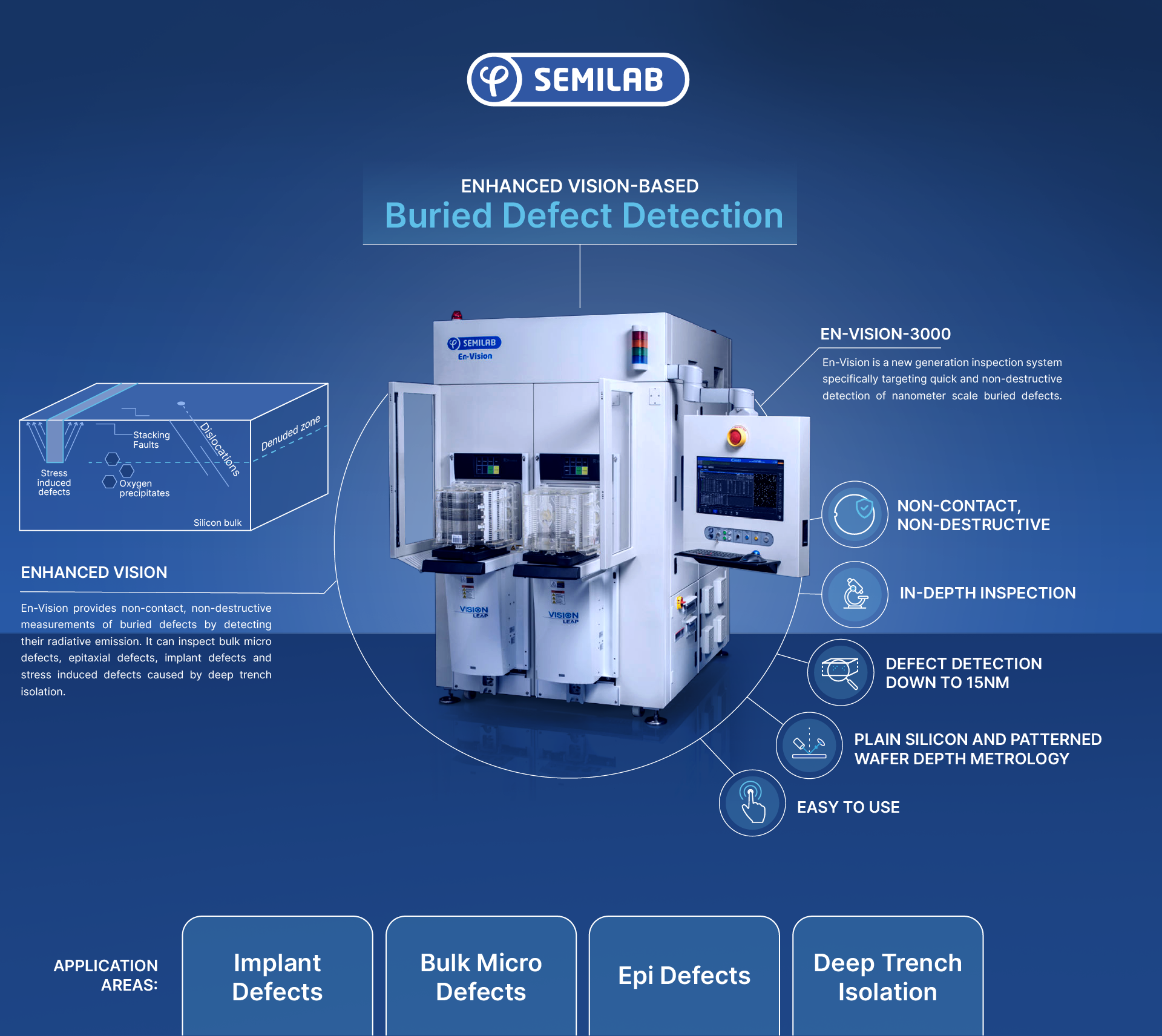
August 18, 2025About the Importance of Quality Control in the Semiconductor Industry and the Possibilities of the Light Scattering Tomography Technique
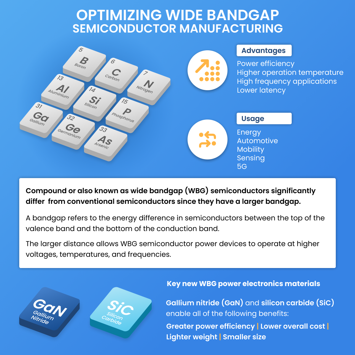
August 18, 2025Wide Bandgap Semiconductors, Their Most Common Industry Usage and What Semilab Can Offer for Compound Material Characterization
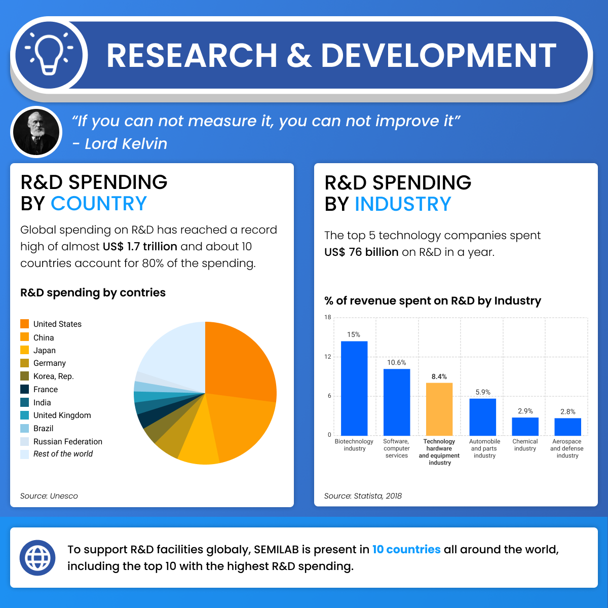
October 17, 2025R&D Keeps The World Moving Forward - So Are Semilab’s Spectroscopic Ellipsometry Solutions