September 17, 2025
Get expert advice and tailored solutions for your research needs
Semilab delivers high-precision characterization tools for R&D in Material and Life Sciences, supporting innovation from nanotechnology to biomedical applications.
Semilab has a strong scientific background and a long history of excellent cooperation with academic customers to develop tailored solutions for R&D applications in the semiconductor, photovoltaic and flat panel display industries, thin film research, materials science, and related scientific disciplines.
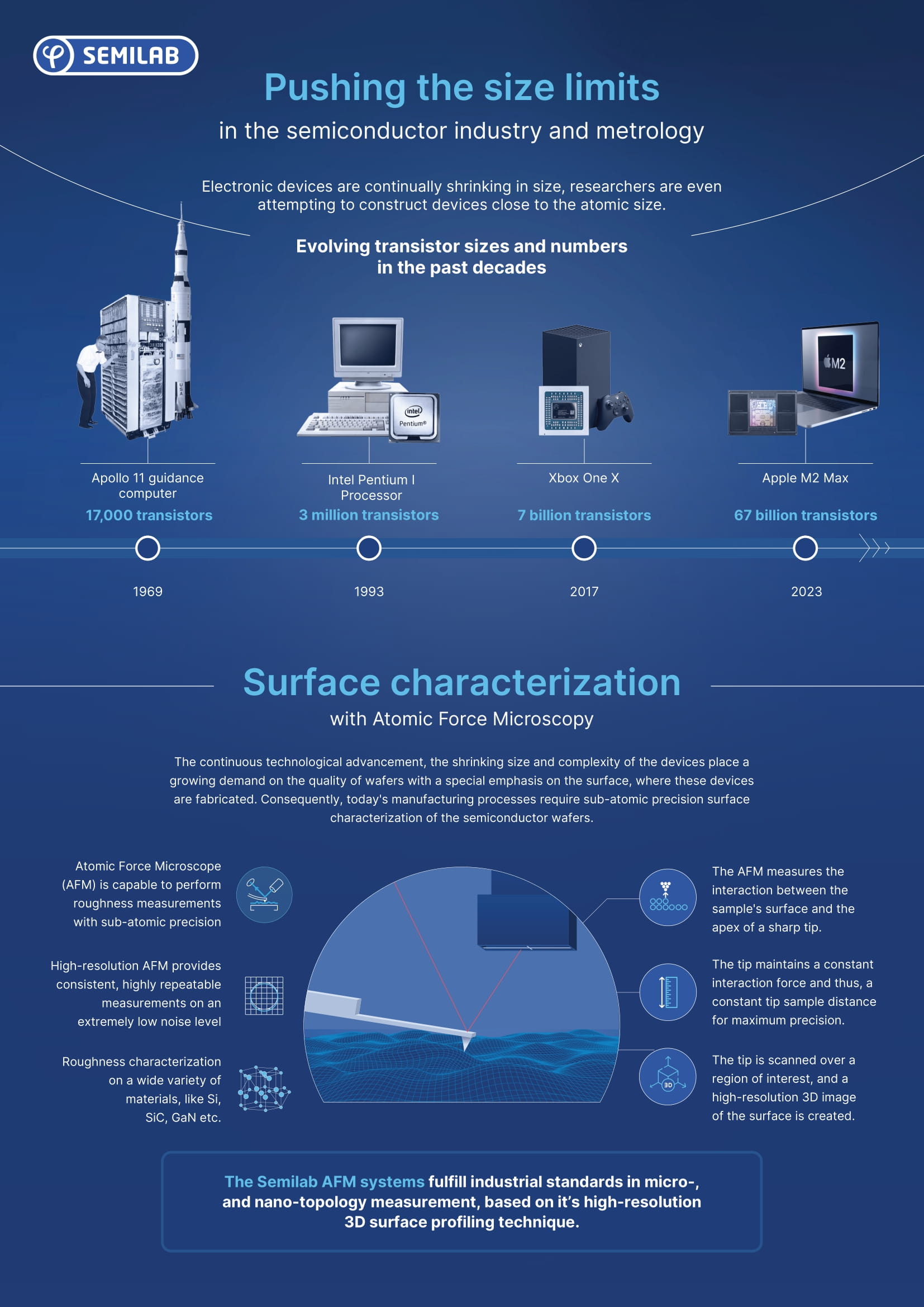
Material Science
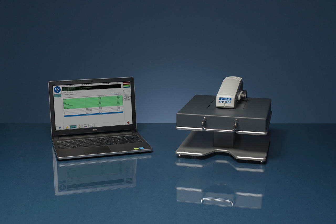
Compact, lab-grade tools for precise electrical resistivity measurement in semiconductor and materials research
Non-contact, high-sensitivity mapping
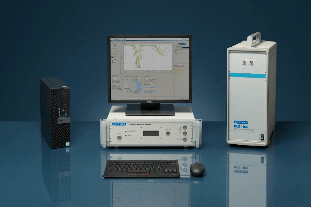
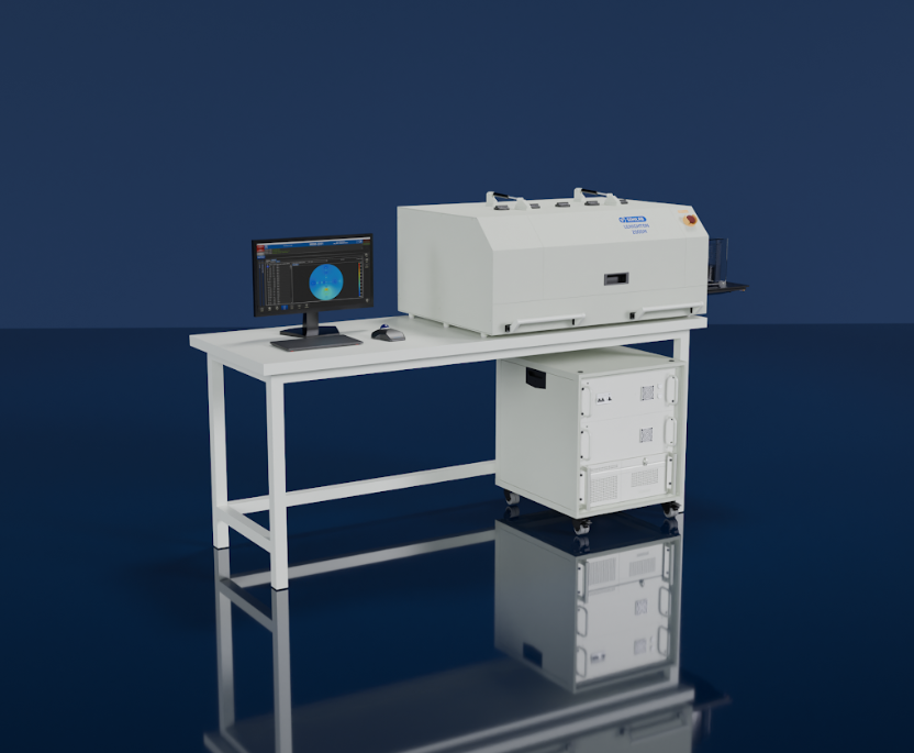
Advanced impurity characterization tools
Accurate thin film analysis
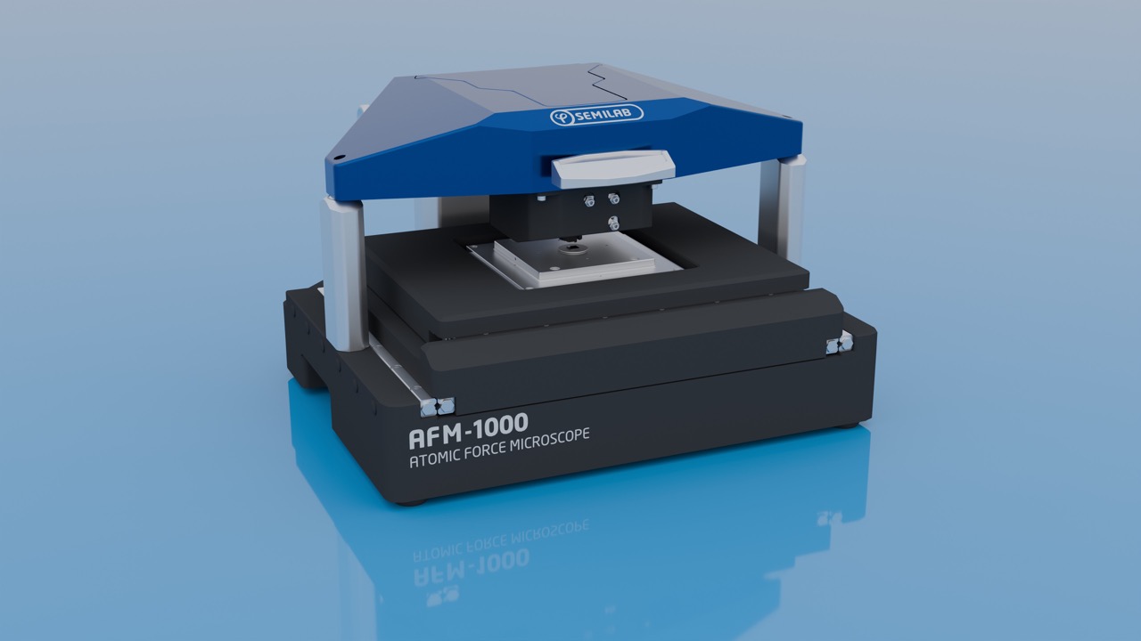
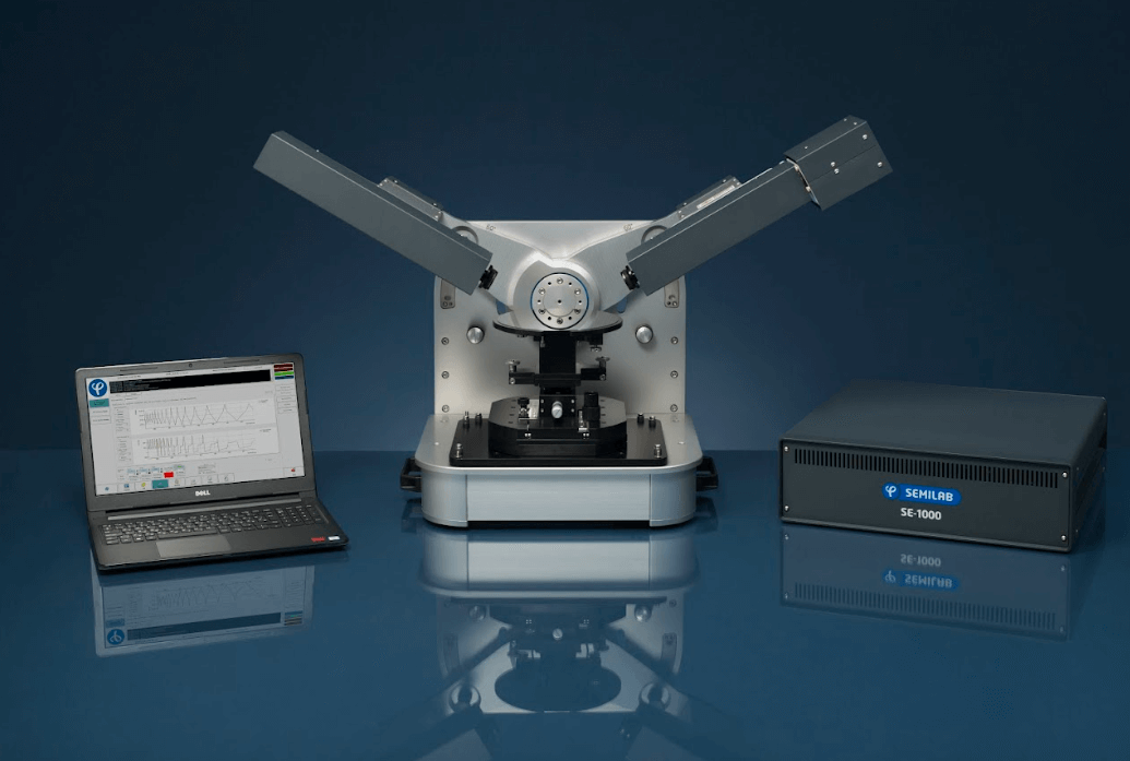
Precision texture and topography mapping
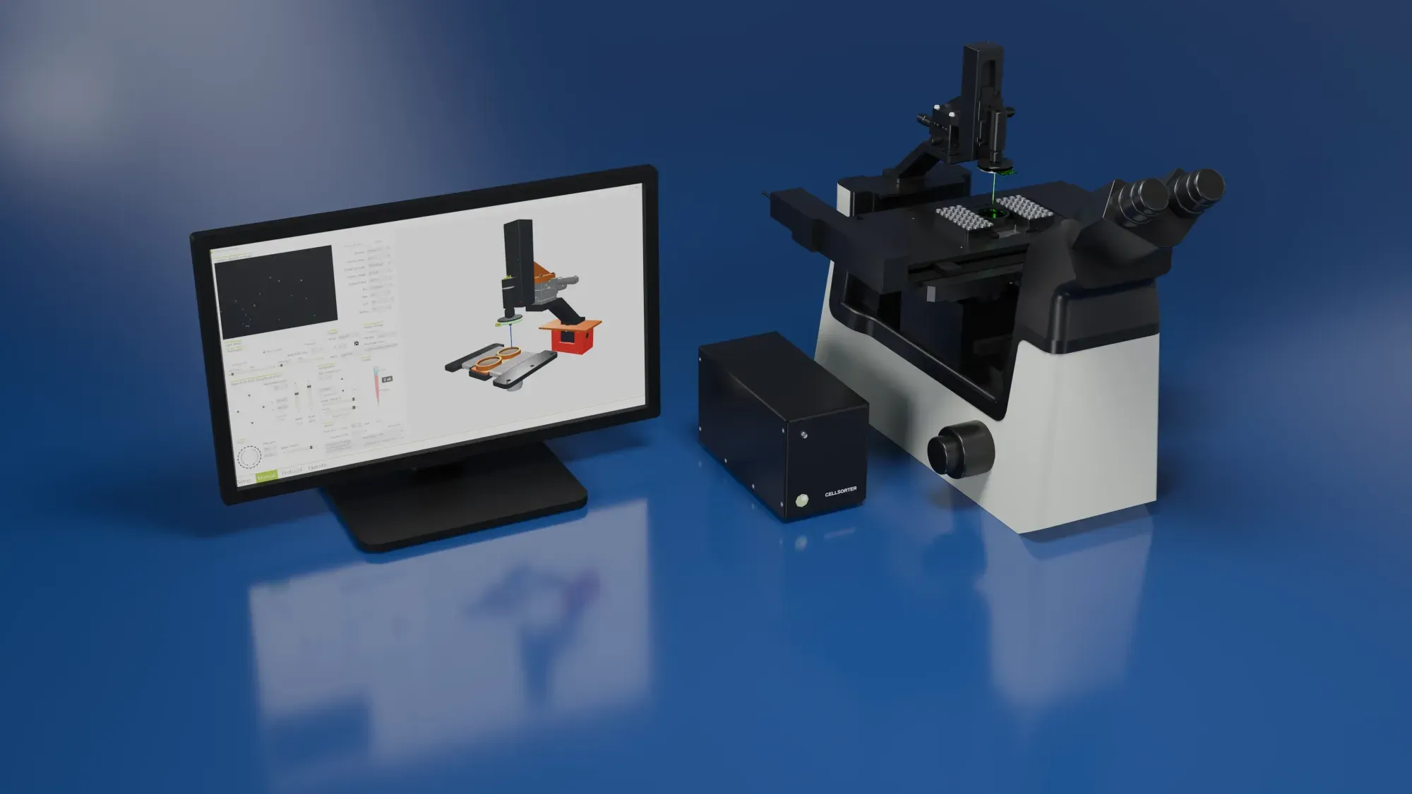
Life Science
Interviews, tips, guides, industry best practices, and news
Read our latest publications
Author: András Bojtor, Dávid Krisztián, Gábor Paráda, Ferenc Korsós, Sándor Kollarics, Gábor Csősz, Bence G. Márkus, László Forró, Ferenc Simon
Topic: Carrier generation & recombination; Metrology; Optoelectronics; Photoconductivity; Radio frequency techniques; Devices; Semiconductors; Microwave techniques
Author: Laszlo Makai, Csaba Balogh, Peter Basa, Jonas Haunschild
Topic: Ellipsometry; Photovoltaics; Monocrystalline textured; TOPCon
Author: Tamás Tarjányi, Csaba Rosztóczy, Ferenc Peták, Fruzsina Kun-Szabó, Gábor Gulyás, József Tolnai, Krisztián Bali, Petra Somogyi, Rebeka Anna Kiss, Gergely H. Fodor
Topic: nanoindentation; diabetes mellitus; rib bone; dynamic loading; aging; IND