Contact us for Information and Pricing
Get expert advice and tailored solutions for your research needs
Get expert advice and tailored solutions for your research needs
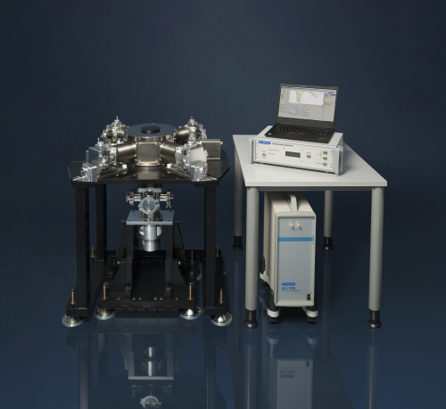
The DLS-1100 is a high-end DLTS system designed for semiconductor R&D and production environments. Featuring an external cryostat for precise temperature control, it offers top-tier sensitivity, full automation, and advanced customization — ideal for production labs, foundries, and high-throughput research facilities.
Author
H-J. Schulze, A. Frohnmeyer, F-J. Niedernostheide, B. Simmnacher, B.O. Kolbesen, P. Tüttő, T. Pavelka, G. Wachutka
Topic
transition metals; contamination; carrier lifetime; silicon defect density
Author
L. Quattropani, K. Solt, P. Niedermann, I. Maggio-Aprile, O. Fischer, T. Pavelka
Topic
Schottky diode; RF plasma treated silicon
Author
C.A. Londos, T. Pavelka
Topic
DLTS; GaAs
Author
D.A. Ramappa, W.B. Henley
Topic
diffusion; iron; silicon dioxide
Author
Homogeneous Transparent Conductive ZnO:Ga by ALD for Large LED Wafers
Topic
GZO; Atomic layer deposition; TCO; Rapid thermal annealing; LED
Author
T. Pavelka and G. Ferenczi
Topic
Thermal emission; deep trap
Author
B. Sandhu, T. Ogikubo, H. Goto, V. Csapó, T. Pavelka
Topic
DLTS; SIRM; Silicon (Si); Mo; Fe; deep levels; carrier lifetime
Author
A. Bertuch, K. Steeples
Topic
NIST traceable; surface photovoltage; standard; reference wafer; Electric measurements; Electrical resistivity; Metrology; Epitaxy; Silicon (Si)
Author
Zsolt Kovács, Csanád Ö. Boros, Teodóra N. Kovács, Zsolt Kovács, ZoltánT. Kiss
Topic
optical inspection; Silicon (Si); POLARIZED INFRARED IMAGING; VISUAL INSPECTION
Author
T. Pavelka and B. Hemm
Topic
Microwave Absorption Spectroscopy
Author
O. Engström, M.Kaniewska, W.Jung, M.Kaczmarczyk
Topic
Deep level transient spectroscopy; quantum dots; tunneling; conduction bands; electric field
August 18, 2025
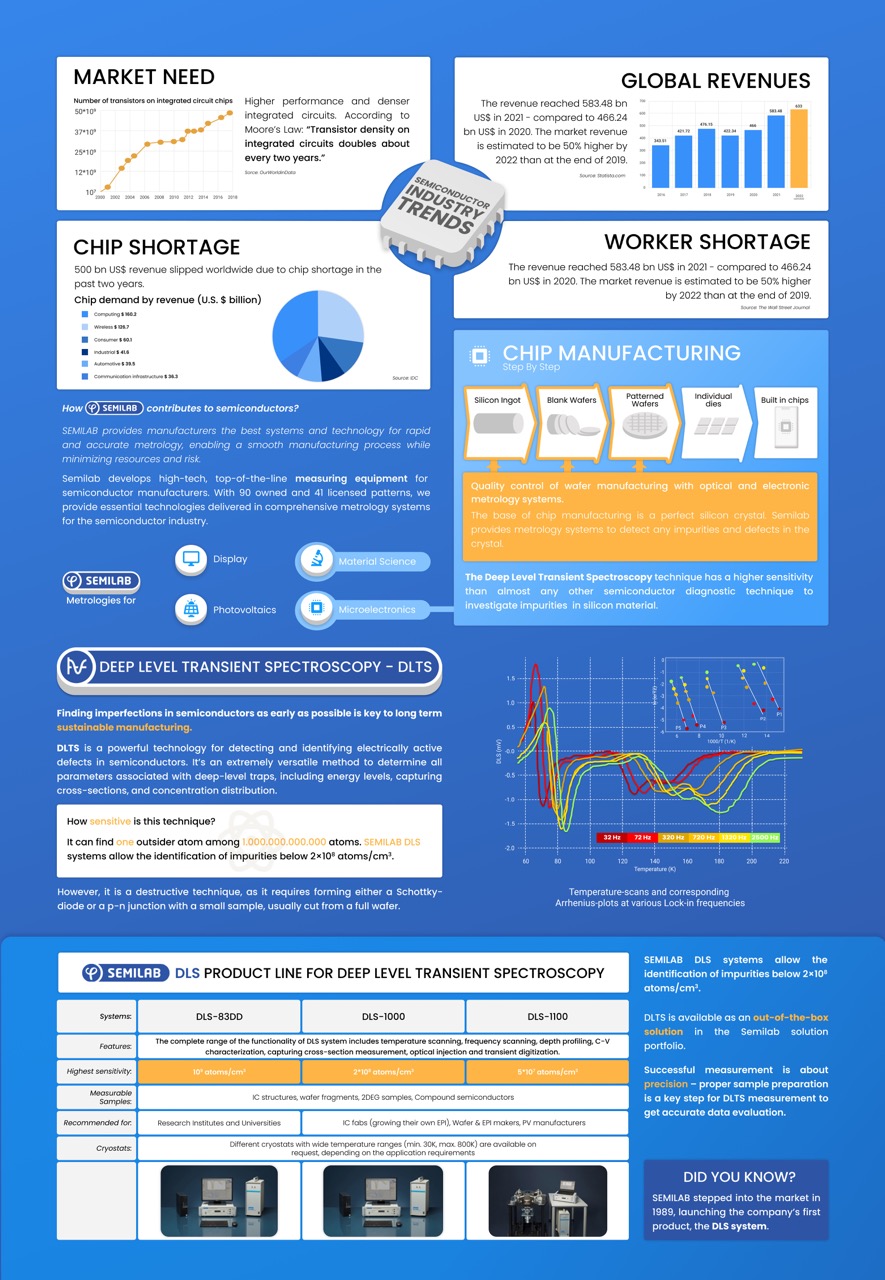
DLTS offers unmatched sensitivity for detecting and analyzing defects in semiconductors, making it a powerful tool for advanced wafer characterization.
August 18, 2025
Uncover the intricacies of your semiconductor samples with precision and confidence and join us in shaping the future of quantum dot technologies and semiconductor excellence.
October 17, 2025
Meeting rising chip demand with precision: How Semilab’s Advanced Metrology takes on complexity in semiconductor manufacturing.
August 18, 2025
Semilab provides DLTS solutions with over 30 years of global experience.