Ferroelectric HfO2 thin film testing and whole wafer mapping with non‐contact corona‐Kelvin metrology
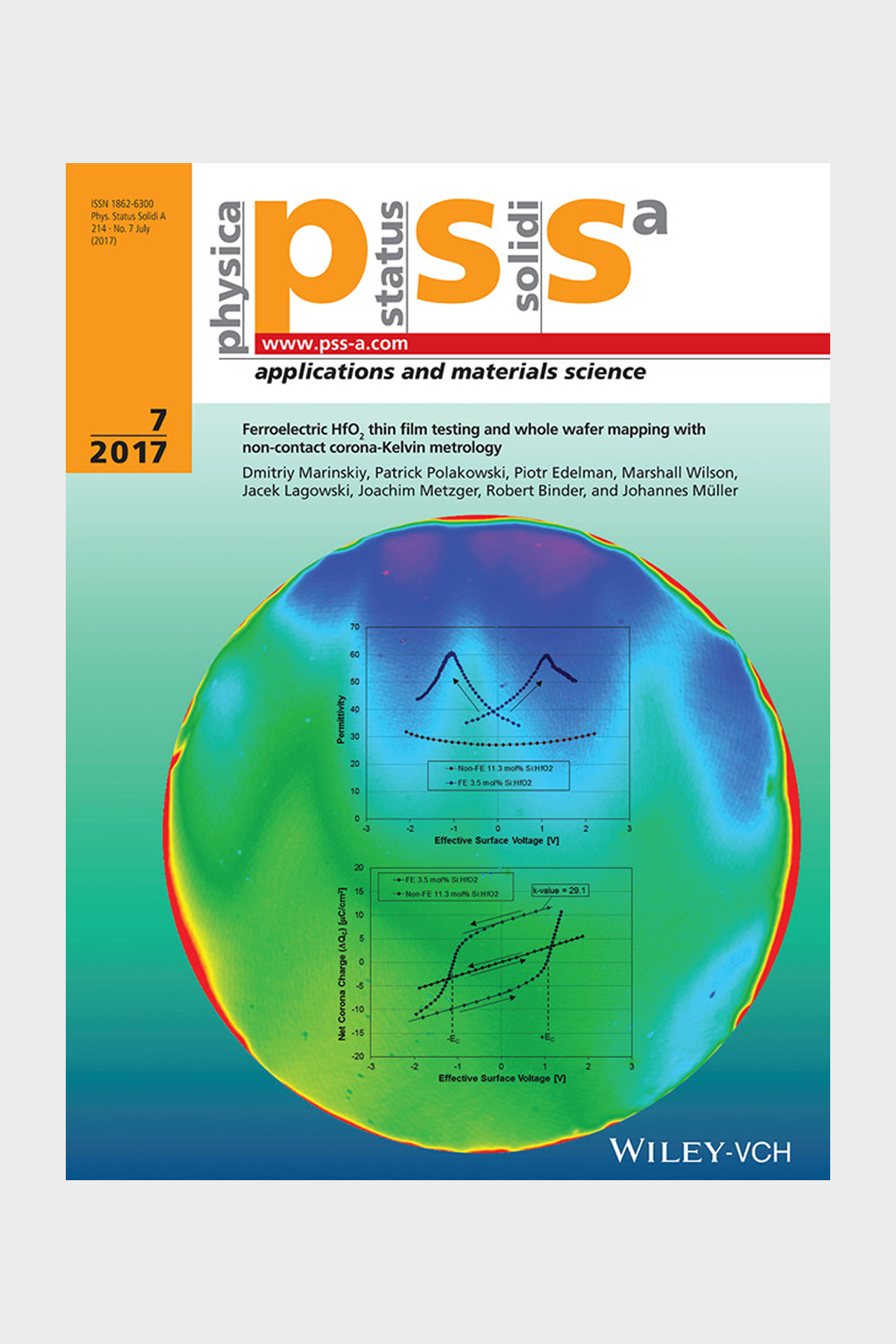
Here, Edelman et al. (article No. 201700249) demonstrate a breakthrough in monitoring ferroelectric properties in thin films that has been achieved using the non-contact corona-Kelvin metrology. As demonstrated by the results on silicondoped HfO2 films, the method enables a noncontact real-time film characterization without the fabrication of capacitor test structures used in the conventional method. The presented approach introduces a corona charge-based method for poling of ferroelectric films. Combined with Kelvin probe measurement of the surface voltage characteristics, the technique enables non-contact monitoring of hysteresis. Such a charge-voltage hysteresis loop and hysteresis of permittivity are shown on the cover image. The results demonstrate ferroelectric behavior in a 3.5mol% Si:HFO2 film and nonferroelectric behavior in a 11.3 mol% Si:HFO2 film. A very important strength of the method is the full wafer mapping for engineering of uniform ferroelectric HfO2 films. The map on the image shows the surface voltage pattern in a Si:HFO2 film, which reflects the laminar wet bench flow pattern after etching of the TiN capping layer.